1Learning Outcomes
Explain how registers can be used to improve throughput performance of a circuit.
Compare how input data is fed through a pipelined circuit and a non-pipelined circuit.
🎥 Lecture Video
In a previous section, we saw an example of where a register was needed to ensure correct circuit behavior. Now, we’ll see how registers can also be used to increase the achievable clock frequency and, thus, improve the performance of the circuit through pipelining [1].
2Adding Registers to Improve Performance
Suppose we had the need to cascade two combinational logic circuits, an adder and a shifter. The idea of this circuit is that, when input values arrive, they are added together and then shifted by some amount. We can imagine that this circuit composition is part of a processor. Figure 1 illustrates this example circuit on the left and timing diagram on the right.
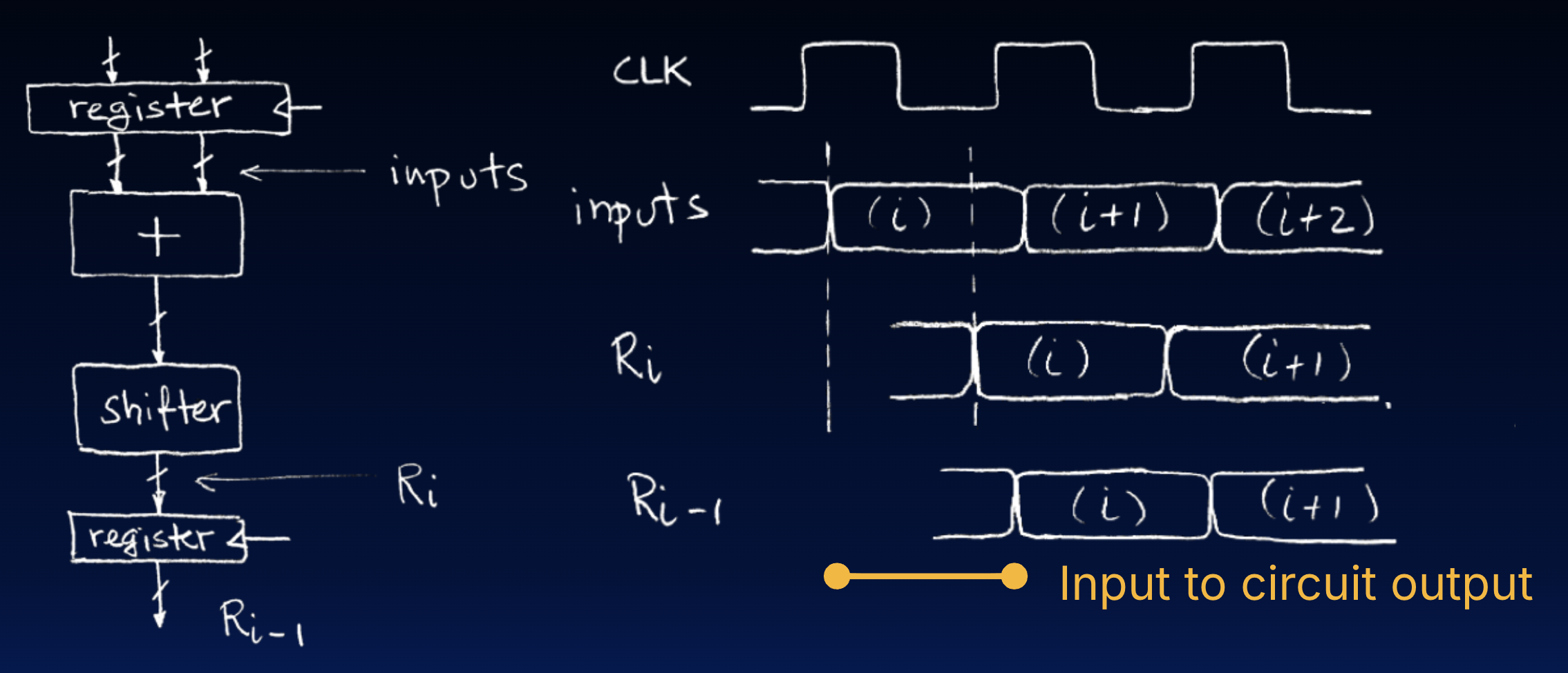
Figure 1:Diagram of a non-pipelined add/shift circuit and the associated timing diagram.
We assume that the input values come from a register (shown in Figure 1 as one combined register block) and the output goes into a register. On each clock cycle, we simultaneously capture a new pair of input values in the input register and the previous result in the output register. The waveforms for the operation of this circuit are shown on the right in Figure 1. There is a delay of one clock cycle from input (output of the input register) to output (output of the output register ).
3Pipelining Registers
The maximum clock frequency (minimum clock period) is limited by the propagation delay of the add/shift operation. If we try to make the clock period too short, then the add/shift logic would not have sufficient time to generate its output. Consequently, the output register would capture an incorrect value.
If we felt that the clock period for the correctly functioning circuit was too long, we could choose to split up the add/shift operation into two cycles, performing the add operation on the first cycle and the shift operation on the second cycle. We can implement this idea by introducing a new register between the two blocks, as shown on the left in Figure 2.
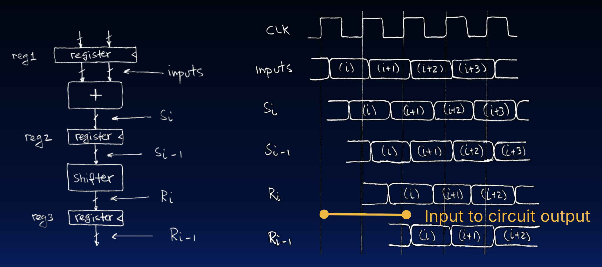
Figure 2:Diagram of a pipelined add/shift circuit and the associated timing diagram.
On each clock cycle, data moves from the output of reg1, through the adder, to the input of reg2, or moves from the output of reg2, through the shifter, to the input of reg3. Since the data no longer needs to move through both blocks in a single clock cycle, the clock frequency can be increased. The waveforms for this pipelined add/shift operation are shown on the right in Figure 2.
There will now be a two clock cycle delay from the insertion of a set of data into the circuit until when it appears at the output. However, the new clock period is shorter, so in absolute time, the delay from data insertion until output is not significantly worse. More importantly, because of the tranformation and the new higher clock rate, results will be generated at a higher rate (more outputs per second). This is a good transformation if you are evaluating on results/time, or throughput! If you are more interested in latency (or delay) for any one set of input values, then this transformation is less ideal.
These notes are adapted from Professor John Wawrzynek’s notes: State Handout.