1And in Conclusion
A finite state machine is a type of simple automaton where the next state and output depend only on the current state and input. Each state is represented by a circle, and every proper finite state machine has a starting state, signified either with the label “Start” or a single arrow leading into it. Each transition between states is labeled [input]/[output]. For example, Figure 1 below is a finite state machine with two states (0 and 1). It outputs 1 when the state changes, and 0 when the state stays the same. The machine starts in state 0. When the input is 0, it stays in its current state and outputs 0. When the input is 1, it switches to the other state and outputs 1. When in state 1, the machine behaves the same way: it stays in state 1 and outputs 0 when the input is 0, and switches back to state 0 with an output of 1 when the input is 1.
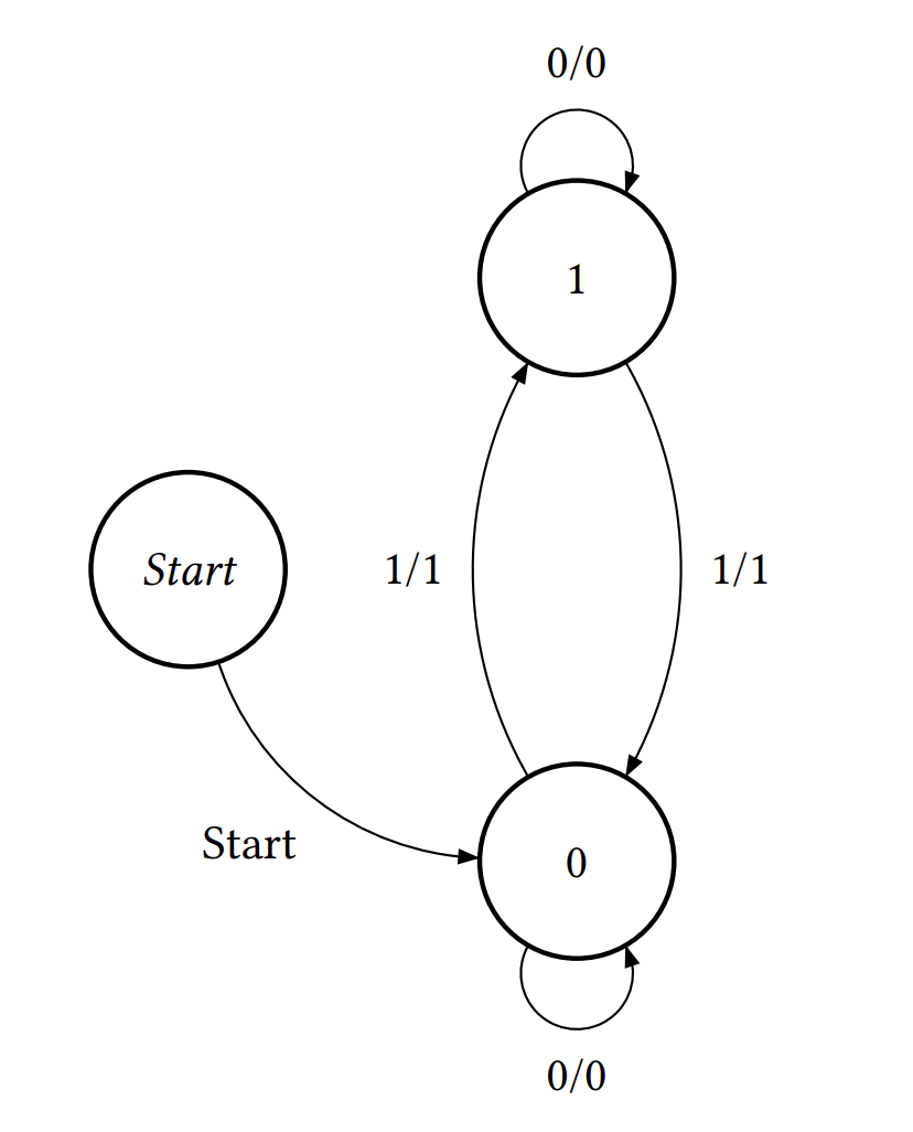
Figure 1:FSM diagram for the description above.
With combinational logic and registers, any FSM can be implemented in hardware!
The input to the register samples has to be stable for a certain amount of time around the rising edge of the clock for the input to be sampled accurately. The amount of time before the rising edge the input must be stable is called the setup time, and the time after the rising edge the input must be stable is called the hold time. Hold time is generally included in clk-to-q delay, so clk-to-q time will usually be greater than or equal to hold time.
Logically, the fact that clk-to-q ≥ hold time makes sense since it only takes clk-to-q seconds to copy the value over, so there’s no need to have the value fed into the register for any longer. Examine the register circuit in Figure 2 and assume setup time of 2.5ps, hold time of 1.5ps, and a clk-to-q time of 1.5ps. The clock signal has a period of 13ps.
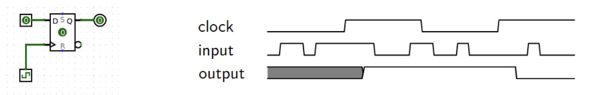
Figure 2:Example register circuit with timing diagram.
Notice that the value of the output in the diagram doesn’t change immediately after the rising edge of the clock. Until enough time has passed for the output to reflect the input, the value held by the output is garbage; this is represented by the shaded gray part of the output graph. Clock cycle time must be small enough that inputs to registers don’t change within the hold time and large enough to account for clk-to-q times, setup times, and combinational logic delays.
A few important SDS relationships are below:
where is the maximum combinational logic delay for any register register path in the circuit. The path with the maximum delay is called the critical path
Additionally, circuits must satisfy hold-time constraints because hold times may be violated if data propagates too quickly:
2Textbook Readings
P&H A.3-A.6
3Additional References
Intro to SDS Handout - Clocks, Delay
State Handout - Registers, FSMs
4Exercises
Check your knowledge!
4.1Conceptual Review
True/False: Register “clk-to-q” delay is the time between the rising edge of the clock signal and the register’s hold time.
Solution
False. “clk-to-q” delay is the time between the rising edge of the clock signal and the time it takes for the register’s output to reflect the new input.
True/False: State elements only update their output on the rising edge of the clock, even if the inputs change between clock rising edges.
Solution
True. State elements will update their output on the rising edge of the clock signal. Between rising edges, the state element’s output will remain constant regardless of the inputs