1Learning Outcomes
Explain why registers help stabilize synchronous systems.
Compute the delay of a circuit’s critical path.
Determine the maximum clock frequency for a given circuit.
Explain a hold time violation and how to avoid it.
🎥 Lecture Video
🎥 Lecture Video
Combination logic circuits produce outputs based purely on their input signals. They are used for a wide variety of functions. State elements, on the other hand, have a small number of very specific uses. These are circuits that remember their input signal values.
2Accumulator Example
Consider the design of a circuit whose job is to form the sum of a list of integers, . Assume that some other circuit applies the numbers from the list one at a time—one per clock cycle. Below is a graphical depiction of an abstraction of our circuit used to form the sum–we’ll call the block “sum”. The values are applied, one per cycle, and after cycles the sum is present at the output, S.
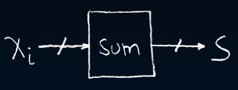
Figure 1:Block diagram for accumulator.
What should we put inside the sum block to achieve the desired function? Obviously the circuit involves an adder. Also, on each step we need to take the current sum and pass it back to the adder so that it can add another X value to it.
2.1Strawman: Unstable Circuit
Figure 2 is our first try:
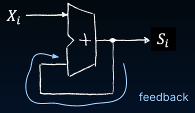
Figure 2:Circuit diagram for accumulator.
Let’s examine the operation of this circuit in detail to see if it does the job. Assume that begins at 0. We then apply . After a short delay (the adder propagation delay, ) will change to . Then after another of delay, S will change to , then after another of delay, S will change to , etc. Because is typically less than the clock period, all of these adds of will happen before is applied.
This is clearly not the correct operation of “sum”. The circuit is out of control! We need some way to control the computation, one step at a time.
2.2Use a Register
The way to control the computation is to put a register in the feedback path (the connection from the output of the adder to its input), as shown in Figure 3.
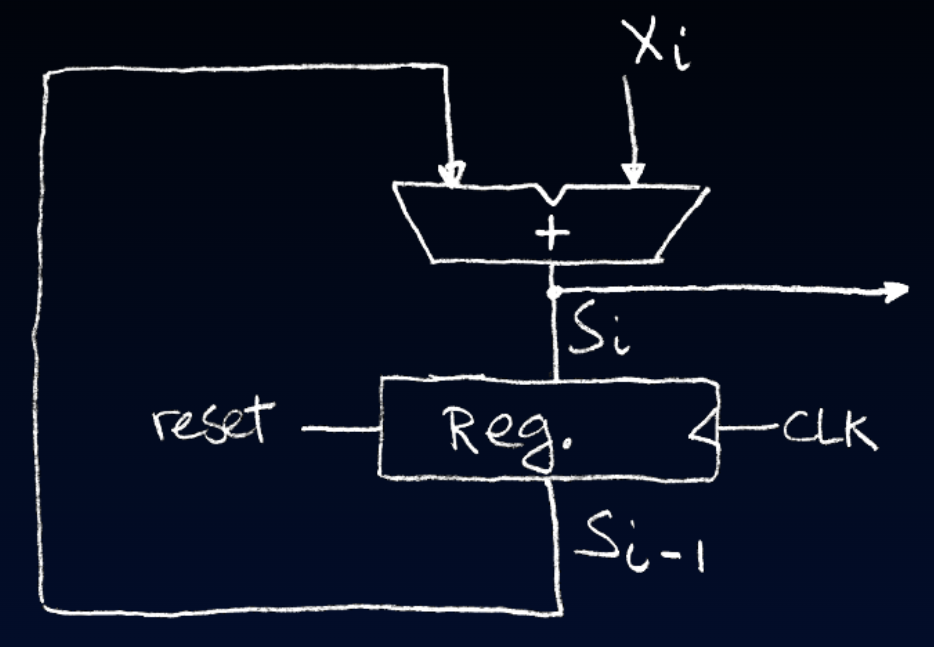
Figure 3:Circuit diagram for accumulator with reset.
The register holds the current value of while the next one is being formed. After we are happy with the next , we load it into the register and apply the new value, then wait for a new to appear at the output of the adder. The process is repeated for all values.
Reset signals are a common feature of register circuits. In the circuit diagram, this is the “reset” input signal to the register. This is a signal that can be used to clear the register value, and thus gives us a way to initialize the circuit.
More on Reset Signals
The “reset” input to the register is a special input that clears the register so that it holds all 0’s.
The most common type of reset input is a called a synchronous reset: If the reset input signal has the value 1 on the rising edge of the clock signal, then the register is cleared, regardless of the value of the input D. In other words, the reset signal has priority over the data input and forces the register to all 0’s.
2.3Waveform diagram
Figure 4 shows the waveforms demonstrating the rough operation of the accumulator circuit, for a few iterations. Results are generated nicely one at time. In this example, the register is used to hold up the transfer of data from one place to another in the circuit.
The output of the circuit is labeled , and the output of the register is labeled to remind us that the register delays the signal for 1 cycle. So if the output of the circuit is holding the result of the ith iteration, then the register holds the result of the (i − 1)th iteration.
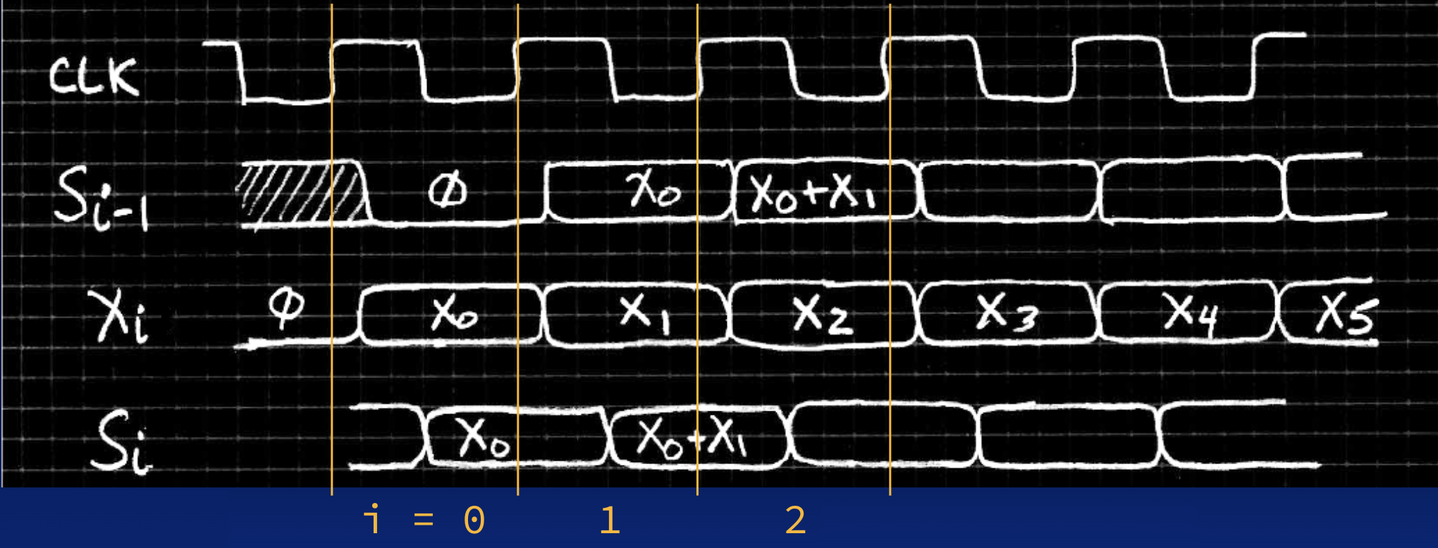
Figure 4:Rough timing diagram for accumulator, now with the waveform for the register output .
Show explanation of Figure 4
Start by looking at the timing of the change on the output of the register . This follows the positive-edge of the clock after a small delay (the clk-to-q time of the flip-flops used to implement the register). We assume that the input is applied at precisely the same time. The two values move through the adder together and after a small delay (the adder propagation delay ) a new result appears at the output of the adder, . Then all is quiet until the rising edge of the clock. At that time the output value is transferred to the register and the whole process repeats.
2.4Different signal arrival times
In practice may not necessarily arrive at the same time as the feedback value, . The waveforms below in Figure 5 show arriving a little bit later than .
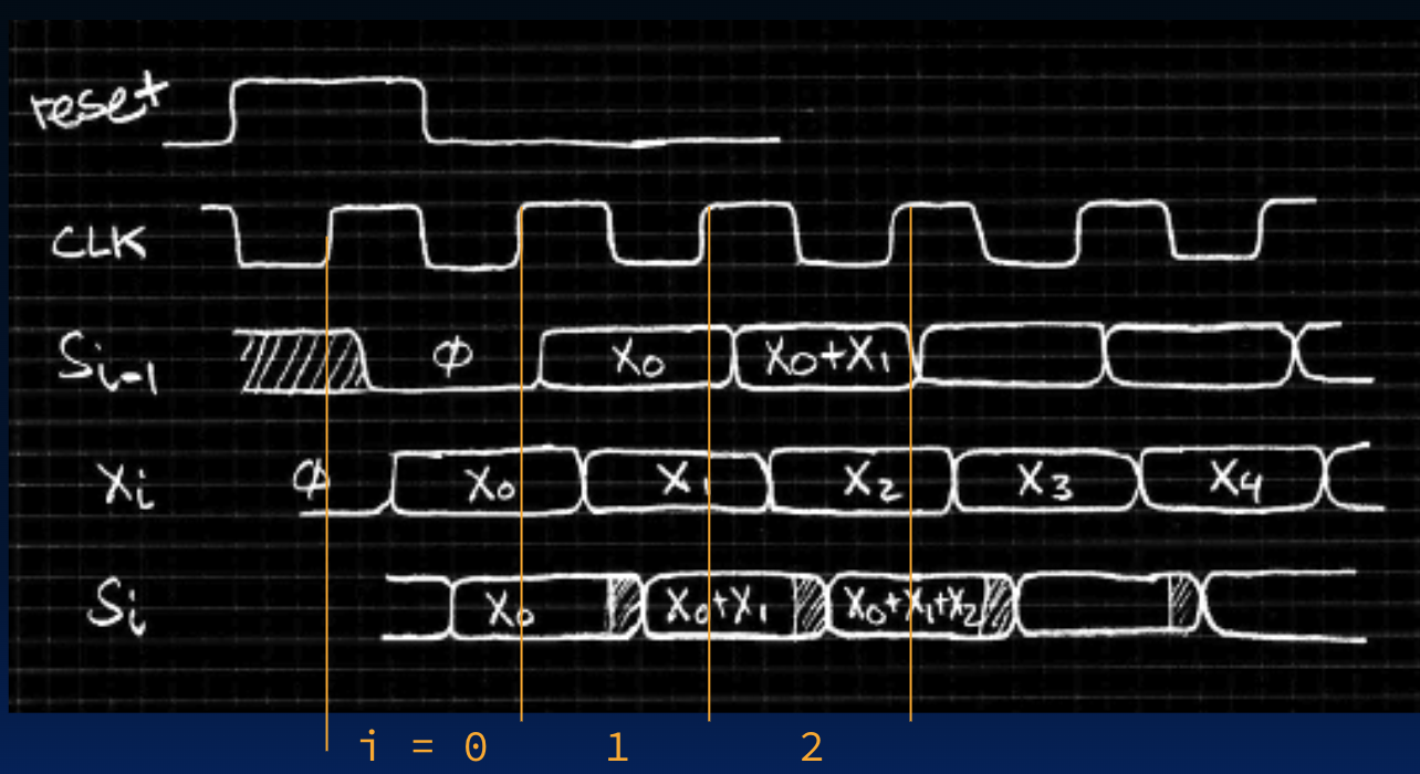
Figure 5:Even though and arrive at different times to the accumulator, the clock period is long enough that is stable before the next rising edge of the clock.
Show explanation of Figure 5
When the register first captures , for a small time period the input still has , therefore the adder begins to compute ! However, this erroneous calculation is quickly aborted when the input changes to . Unfortunately, the aborted computation will probably make it through the adder, creating a sort of instability at the output. However, the instability in has no effect on , as it captures its value from before it goes bad.
As seen above, on each cycle there is a small time period where the adder has inconsistent inputs. This sort of arrival mismatch and subsequent output instability is common in many circuits. In properly designed circuits, this instability never happens around the rising-edge of the clock and therefore gets ignored by the registers and downstream circuitry.
3Computing Maximum Clock Frequency
Notice that the maximum clock frequency (minimum clock period) is limited by the propagation delay of the add/shift operation. If we try to make the clock period too short, then the add/shift logic would not have sufficient time to generate its output and the output register would capture an incorrect value.
At thge same time, we seek to create high-bandwidth circuits, which produce many outputs per second. We’d like to find an ideal balance between a high-frequency clock and stable outputs.
Figure 6 shows a typical circuit.
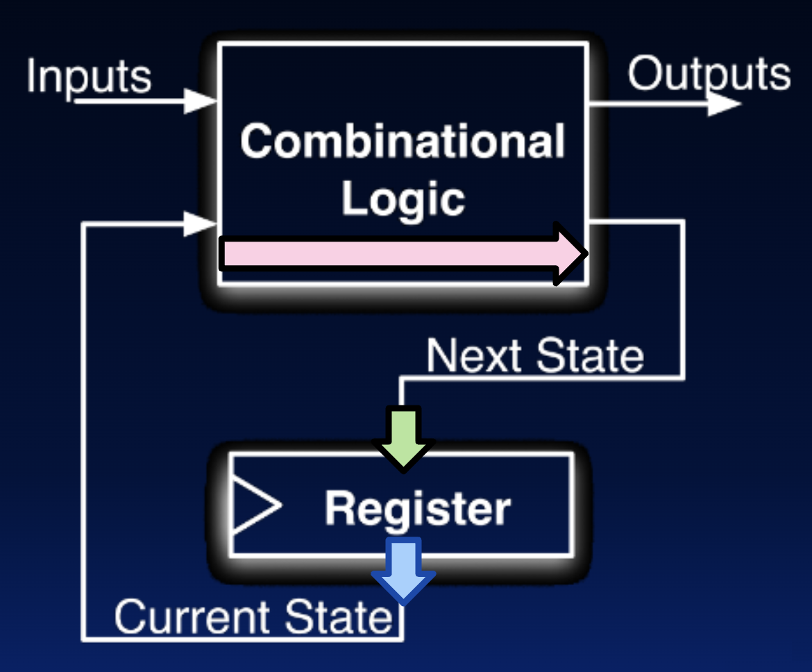
Figure 6:To determine the minimum clock period, compute the delay on the critical path.
In this circuit, the critical path is:
where clk-to-q delay and setup time are properties of the register (e.g., internal flip flops), and CL delay is the delay through the combinational logic block.
Show Answer
4Hold Time Violations
Above, the critical path determins the maximum clock frequency we can use to ensure a stable input to our register elements. We next present a different problem: hold time violations.
Recall from earlier that the hold time is the duration during which a register’s input d must be stable after the rising edge of the clock. There are some cases where data propagates through the circuit is so fast that the input to registers become unstable during the hold time.
While rare[1], this may occur if the best-case delay between clocked elements is shorter than the hold time. To mitigate this, we could add arbitrary delay to combinational logic the circuit to increase the best-case delay.
See the relevant footnote in a previous section.